
PCB Fabrication Services

PCB fabrication is where an electronics product becomes real hardware. For engineering teams, procurement teams, and EMS/ODM partners, the key concern is not only getting a board produced—it’s getting a board produced correctly, with stable process control, predictable assembly results, and documentation that supports production confidence.
At Shenzhen HiFlexlink Technology Co.,Ltd., we support engineering-focused PCB fabrication for projects ranging from prototypes to production-ready manufacturing. We work with advanced interconnect requirements, including 4–20 layer multilayer PCBs, HDI PCBs, and rigid-flex PCBs. We also support major surface finish options such as ENIG, OSP, Immersion Tin, HASL, and ENEPIG, so your boards match your assembly process and reliability goals.
his page is designed to help you quickly understand:
- what a professional PCB manufacturing process looks like end-to-end
- which PCB types fit different design needs
- how to choose surface finishes for assembly reliability
- what files are needed for a fast PCB fabrication quote
- how quality and reliability are supported through inspection and verification
Why PCB Fabrication Planning Impacts Reliability and Yield
When a PCB is fabricated with inconsistent process control or incomplete file interpretation, downstream assembly problems can happen—such as solderability variations, misregistration between layers, or reliability risks in dense via structures.
A reliability-oriented PCB fabrication service typically emphasizes:
- DFM risk reduction before fabrication starts
- stable imaging/etching and lamination control for multilayer boards
- via formation and plating quality for electrical interconnect reliability
- solder mask registration and clearance consistency for safe assembly
- surface finish selection aligned to reflow and storage window
- inspection checkpoints and verification records aligned with your scope
At Shenzhen HiFlexlink Technology Co.,Ltd., we position our support around engineering practicality: helping you reduce uncertainty early, clarify file requirements, and coordinate fabrication planning toward predictable results.
PCB Fabrication Capabilities (4–20 Layers, HDI, Rigid-Flex)
Our capability focus covers multilayer PCB fabrication in the 4–20 layers range. For advanced designs, we also support HDI and rigid-flex requirements. Depending on the project scope, we can coordinate qualified manufacturing partners to meet specific structural needs.
Table 1 — PCB Types & When to Choose Them
| PCB Type | Typical Project Scenarios | Why It’s Chosen | Manufacturing Focus (Reliability Angle) |
|---|---|---|---|
| Single-layer | Basic prototypes, low interconnect density | Low cost, quick turnaround | Pattern definition, solder mask registration |
| Double-layer | General electronics, straightforward routing | Reliable and cost-efficient | Etching accuracy, drill/via quality |
| Multilayer (4–20 layers) | Complex routing, compact integration | More routing layers in smaller footprint | Lamination stability, alignment control, via reliability |
| HDI PCB | High-density electronics, compact modules | Enables fine pitch routing and advanced via strategies | Microvias, via formation control, DFM verification |
| Rigid-Flex PCB | Space-saving mechanical integration | Reduces connectors/cabling and improves fit | Layer-to-flex bonding and reliability-focused process control |
Surface Finishes for Assembly Reliability (ENIG / OSP / Immersion Tin / HASL / ENEPIG)
A surface finish is not just a cosmetic choice. It influences:
- solderability at the time of assembly
- reflow behavior and wetting
- storage stability before assembly
- long-term reliability for mission-critical electronics
We support major finish options including:
- ENIG (Electroless Nickel Immersion Gold)
- OSP (Organic Solderability Preservative)
- Immersion Tin
- HASL (lead-free/lead options as required by program)
- ENEPIG (Electroless Nickel Electroless Palladium Immersion Gold)
If you’re not sure which finish to choose, share your assembly timeline and expected storage duration—we can help guide a manufacturable, reliability-oriented selection.
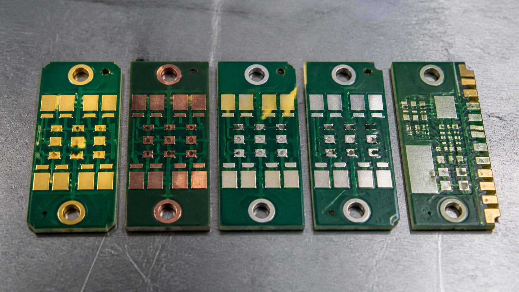
Table 2 — Surface Finish Comparison (Practical Selection Guide)
| Surface Finish | Key Benefits | Assembly Considerations | Typical Fit |
|---|---|---|---|
| ENIG | Good solderability and reliable wetting | Often favorable for fine-pitch SMT | High-value electronics, controlled assembly timelines |
| OSP | Cost-effective protection | Best when assembly occurs within expected window | Prototypes and fast-turn production |
| Immersion Tin | Widely used, good solderability | Storage time and handling matter | General SMT/THT workflows |
| HASL | Broad compatibility | Surface consistency varies by process | Through-hole + mixed assembly (program dependent) |
| ENEPIG | Enhanced reliability-focused stack | Designed for specific long-term performance goals | Projects with strict reliability expectations |
Our PCB Fabrication Process (From Files to Final Boards)
A dependable PCB manufacturing process is repeatable and engineering-driven. While exact steps can vary depending on PCB type and requirements, a reliability-oriented workflow typically includes file review, inner-layer processing, lamination, via formation, solder mask application, finishing, and final inspection.
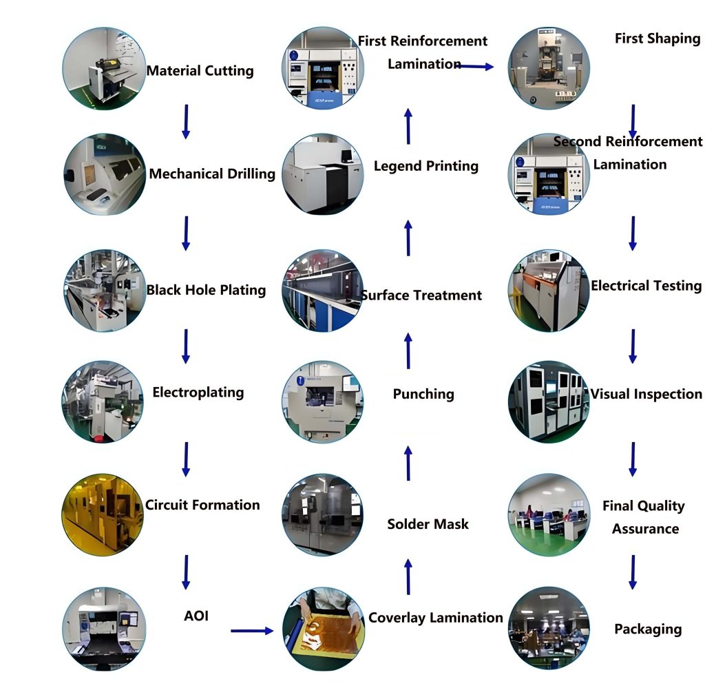
Table 3 — PCB Fabrication Process Steps & Typical Outputs
| Process Stage | What It Does | Key Outputs | Why It Matters for Reliability |
|---|---|---|---|
| 1) DFM & File Review | Check manufacturability from files | Risk list, parameter confirmation | Prevents rework, misalignment, and yield loss |
| 2) Inner Layer Imaging/Etching | Create internal copper patterns | Inner layer copper geometry | Accuracy supports layer-to-layer alignment |
| 3) Lamination (Multilayer) | Bond stack-up layers | Stable multilayer structure | Impacts planarity and interconnect reliability |
| 4) Via Formation & Plating | Create vertical interconnects | Via walls, plated interconnects | Via reliability is critical in HDI/multilayer designs |
| 5) Outer Layer Patterning | Define traces, pads, outline | Trace/pad structures and edge definition | Determines solderability and assembly performance |
| 6) Solder Mask Printing & Curing | Protect copper and define openings | Mask coverage + registration | Reduces short risk and supports consistent solder joints |
| 7) Surface Finish & Marking | Apply finishing and identification | Finish-ready pads and markings | Solderability and storage behavior depend on this stage |
| 8) Final Testing & QC | Verify scope-based targets | Inspection records, QA sign-off | Confirms boards match requirements before shipping |
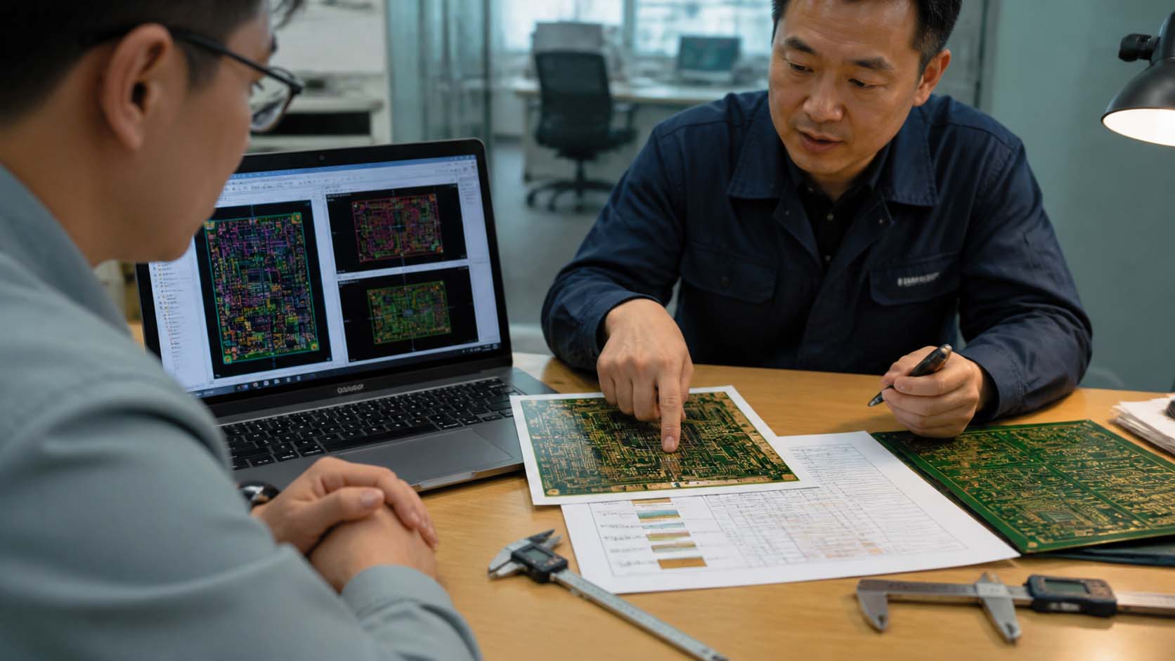
DFM Review — Reduce Risk Before Fabrication Starts
An engineering-minded DFM review for PCB fabrication focuses on whether your files translate correctly into manufacturable layers and reliable interconnects. Typical topics include:
- design rule feasibility and critical feature interpretation
- via and drill parameters affecting reliability
- solder mask openings and pad geometry consistency
- layer count and stack-up considerations for multilayer designs
- any special structural considerations for HDI and rigid-flex layouts
FM is not about rejecting designs—it’s about reducing uncertainty early.
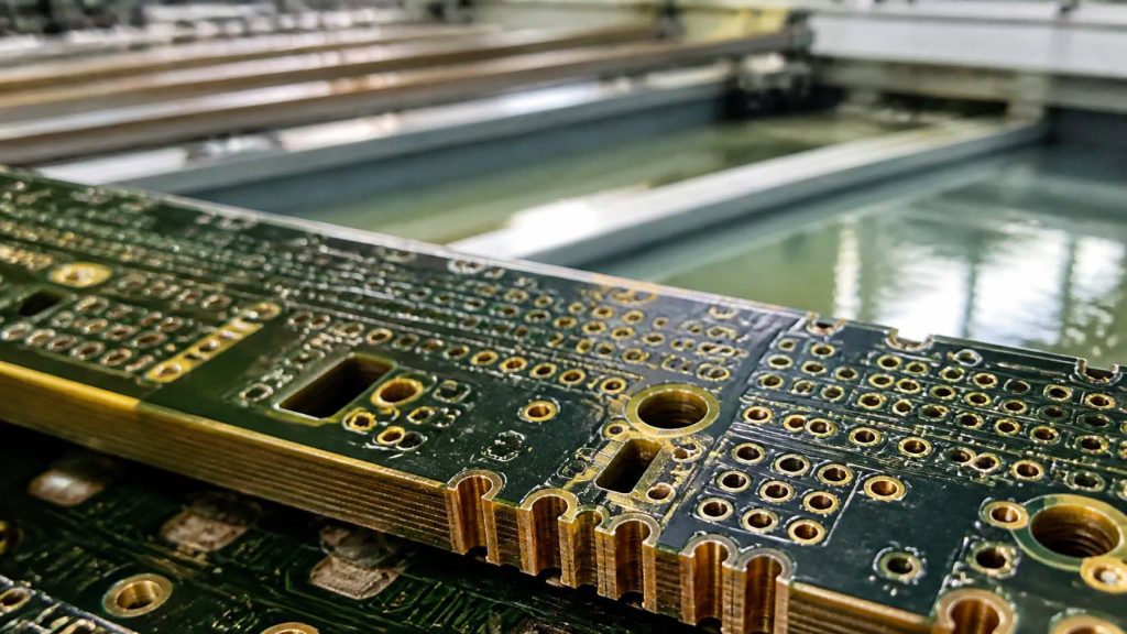
Via Formation & Plating — Reliability in Dense Designs
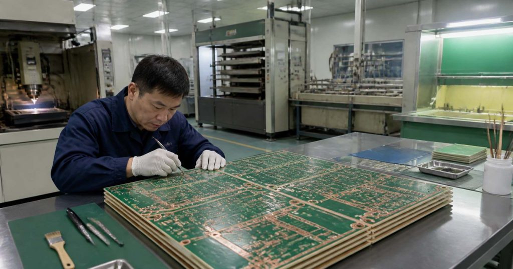
For multilayer, HDI, and many rigid-flex applications, via reliability is a critical factor. A reliability-focused fabrication workflow emphasizes stable via formation and controlled plating to support:
- consistent electrical interconnect continuity
- predictable via wall quality
- repeatable assembly outcomes
If your design includes dense via structures, a DFM-aligned file review becomes even more important.
Solder Mask and Surface Finish — Make Assembly Predictable
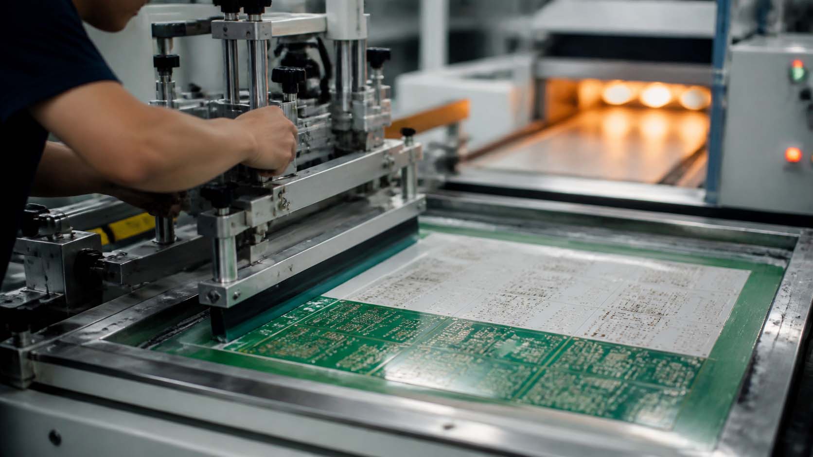
During assembly, solderability and solder joint quality strongly depend on:
- solder mask registration and clearance around pads
- surface finish behavior during reflow
- storage window alignment prior to component placement
We support solder mask and finishing workflows intended to improve assembly safety and yield predictability—especially for advanced boards.
Quality & Reliability Evidence (Process Control + Inspection)
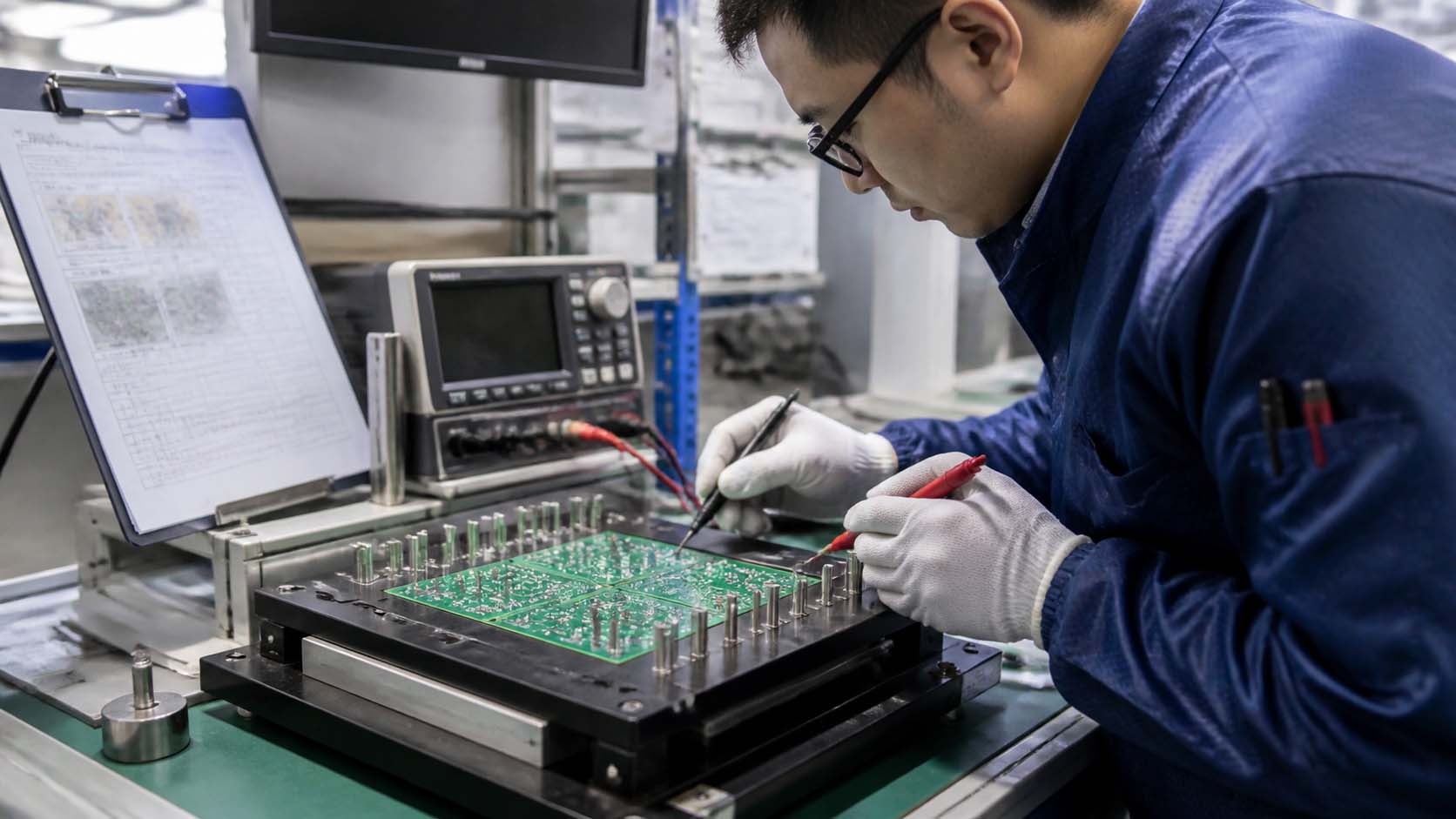
Because your priority is reliability and engineering confidence, we can support a scope-aligned quality approach. Depending on project requirements, typical reliability evidence may include:
- Process control evidence
- QC checkpoints across major steps (imaging/etching, lamination, plating, mask, finishing)
- Inspection and verification
- visual inspection aligned with mask/legend/pad conditions
- electrical/continuity checks within agreed scope
- dimensional checks for critical features
- Compliance support
- RoHS/REACH-related expectations as required for the program
- Traceability and documentation
- inspection and QA records aligned to customer internal review needs
If you have a specific acceptance criteria format, we can align our workflow to your requirements.
What Files You Need for a PCB Fabrication Quote
To quote accurately and minimize iteration, send a complete fabrication file package. Typically, we request:
Table 4 — PCB Fabrication Quote File Requirements
| Required Item | Typical Format | Why It’s Needed | Notes |
|---|---|---|---|
| Gerber files | RS-274X | Defines layers, copper, solder mask, legends | ODB++ may be acceptable depending on workflow |
| NC drill files | Excellon format | Defines drilling locations and sizes | Drill sizes and tolerances affect reliability |
| Board outline | Included in Gerbers or separate outline | Supports panelization and dimension control | Specify thickness and tolerance needs |
| Stack-up / layer count | Notes or from design stack-up | Confirms feasibility for 4–20 layers | Especially important for HDI/rigid-flex |
| Surface finish preference | ENIG / OSP / Immersion Tin / HASL / ENEPIG or “recommend” | Impacts solderability and process route | Storage time influences finish recommendation |
| Quantity + target lead time | Number of pieces/panel | Scheduling and cost planning | Prototype vs production timing considerations |
| Special requirements | Text notes | Defines test scope, acceptance criteria, and constraints | Include impedance control if applicable |
Lead Time for PCB Fabrication (Prototype to Production)
PCB fabrication lead time depends on:
- layer count (4–20 layers)
- PCB structure complexity (multilayer, HDI, rigid-flex)
- surface finish selection (ENIG/OSP/Immersion Tin/HASL/ENEPIG)
- queue and scheduling
- the scope of inspection/testing aligned with your needs
After reviewing your files, we can provide a structured plan for scheduling and lead time expectations.
Request a PCB Fabrication Quote
If you want a clear, engineering-oriented PCB fabrication experience, prepare your Gerber and NC drill files, specify your layer count/stack-up needs, and share your preferred surface finish (or ask us to recommend). We will support DFM-oriented risk reduction and fabrication planning toward reliable results.
Contact us to request a PCB fabrication quote for your multilayer, HDI, or rigid-flex project.
FAQ — PCB Fabrication (Engineering Questions)
What is PCB fabrication?
PCB fabrication is the manufacturing workflow that converts design files into physical printed circuit boards, typically including imaging/etching, lamination, plating, solder mask application, surface finishing, and final QC/testing.
Can you support HDI and rigid-flex PCB fabrication?
Yes. HDI PCB fabrication and rigid-flex manufacturing can be supported. Because advanced structures require careful parameter planning, we recommend DFM-oriented file review before scheduling.
Do you support ENIG, OSP, Immersion Tin, HASL, and ENEPIG?
Yes. We support multiple surface finish options including ENIG, OSP, Immersion Tin, HASL, and ENEPIG. The best choice depends on your assembly timeline and reliability goals.
What files should I send for a PCB fabrication quote?
Please send Gerber files and NC drill files (Excellon format). If available, include stack-up information, board outline details, quantity, target lead time, and surface finish preference.
Do you provide DFM review support?
Yes. We can provide a DFM-oriented file review to identify manufacturability risks early and help reduce iteration and production delays.
What quality and reliability evidence can you support?
Quality control scope depends on your project requirements. We can support process-controlled manufacturing steps, inspection checkpoints, and verification within agreed scope, with documentation aligned to customer internal approval needs.